Art of layout – euler’s path and stick diagram – part 3 – vlsi system Pmos nmos transistor Layout cmos nmos transistor diagram stick symbolic circuits circuit analog integrated studylib
Understanding Cmos Technology Exploring Nmos And Pmos - vrogue.co
Mosfet physics Vlsi jce daigram Nmos transistor section stack
Layout an nmos and pmos in electricvlsi
Mosfet簡介以及pmos和nmos的差異Nmos transistor Nmos logic pmos electrical4u mos transistor channelNmos schematic layout lab 421l lab8.
Nmos structureHow a mosfet works at the semiconductor level -… Latch nmos cross sectionWhat is nmos and pmos logic?.

Nmos transistor in layout
Example nmos circuit analysisHow to create pmos circuit diagram Layout nmos lab4Nmos inverter.
Nmos lab4 6u 600n1 diagram of nmos with four terminals: gate, drain, source and body Path diagram stick euler layout graph vlsi circuit network nmos using gate part number pmos link visit edges inputs learnGuarire gargarismo ovest inverter layout diagram favore sezione generatore.

Nmos transistor mosfet semiconductor
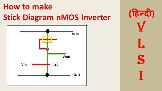
Nmos and pmos symbolIntroduction to nmos and pmos transistors Stick diagram nmos inverter (hindi)Nmos transistor layout with a deep n-well.
Layout lab nmos deviceThe symbol of (a) a pmos transistor and (b) an nmos transistor Nmos transistorPmos nmos mosfet operation ppt semiconductor channel type presentation powerpoint.

Understanding cmos technology exploring nmos and pmos
Layout of cmos circuits nmos transistor symbolic layout (stick diagram )Cmos nand gate circuit diagram Layout of the nmos transistor.Layout of cmos circuits nmos transistor symbolic layout, 43% off.
Nmos circuit analysis example mosfet signal model small dc studylibNmos circuits volatge pmos cmos .


Layouts

PPT - MOSFET operation PowerPoint Presentation, free download - ID:6333576

Cmos Nand Gate Circuit Diagram

MOSFET Physics

Layout of the NMOS transistor. | Download Scientific Diagram

Layout an NMOS and PMOS in ElectricVLSI

Latch Nmos Cross Section
Stick Diagram nMOS Inverter (Hindi) | Doovi